- 您现在的位置:买卖IC网 > Sheet目录1251 > UM245R (FTDI, Future Technology Devices International Ltd)MOD USB PARALLEL FIFO DEV FT245R
�� �
�
�Document� Reference� No.:� FT_000202�
�UM245R� USB� -� Parallel� FIFO� Development� Module� Datasheet� Version� 1.04�
�Clearance� No.:� FTDI#� 124�
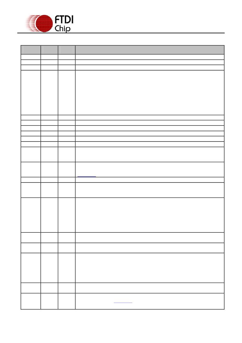
�4.2� Signal� Descriptions�
�Pin� No.�
�1�
�2�
�3�
�4�
�Name�
�DB0�
�DB4�
�DB2�
�VIO�
�Type�
�I/O�
�I/O�
�I/O�
�PWR�
�Description�
�FIFO� Data� Bus� Bit� 0*�
�FIFO� Data� Bus� Bit� 4*�
�FIFO� Data� Bus� Bit� 2*�
�+1.8V� to� +5.25V� supply� to� the� FIFO� Interface� and� Control� group� pins� (1...3,� 5,� 6,�
�9...14,� 22,� 23).�
�In� USB� bus� powered� designs� connect� to� 3V3OUT� to� drive� out� at� 3.3V� levels� (connect�
�jumper� J1� pins� 1� and� 2� together),� or� connect� to� VCC� to� drive� at� 5V� CMOS� level� (connect�
�jumper� J1� pins� 2� and� 3� together).� This� pin� can� also� be� supplied� with� an� external� 1.8V� –�
�5.0V� supply� in� order� to� drive� at� different� levels.� It� should� be� noted� that� in� this� case� this�
�supply� should� originate� from� the� same� source� as� the� supply� to� Vcc.� This� means� that� in�
�bus� powered� designs� a� regulator� which� is� supplied� by� the� 5V� on� the� USB� bus� should� be�
�used.�
�5�
�6�
�7,� 24�
�8�
�9�
�10�
�11�
�DB1�
�DB7�
�GND�
�DB5�
�DB6�
�DB3�
�PWE#�
�I/O�
�I/O�
�PWR�
�I/O�
�I/O�
�I/O�
�I/O�
�FIFO� Data� Bus� Bit� 1*�
�FIFO� Data� Bus� Bit� 7*�
�Module� ground� supply� pins�
�FIFO� Data� Bus� Bit� 5*�
�FIFO� Data� Bus� Bit� 6*�
�FIFO� Data� Bus� Bit� 3*�
�Goes� low� after� the� device� is� configured� by� USB,� then� high� during� USB� suspend.� Can� be�
�used� to� control� power� to� external� logic� P-Channel� logic� level� MOSFET� switch.� Enable� the�
�interface� pull-down� option� when� using� the� PWREN#� pin� in� this� way.�
�12�
�RD#�
�I/O�
�Enables� the� current� FIFO� data� byte� on� D0...D7� when� low.� Fetched� the� next� FIFO� data�
�byte� (if� available)� from� the� receive� FIFO� buffer� when� RD#� goes� from� high� to� low.� See�
�Section 4.4� for� timing� diagram.*�
�13�
�14�
�SLD�
�USB�
�GND�
�Output�
�USB� Cable� shield.�
�5V� Power� output� USB� port.� For� a� low� power� USB� bus� powered� design,� up� to� 100mA� can�
�be� sourced� from� the� 5V� supply� on� the� USB� bus.� A� maximum� of� 500mA� can� be� sourced�
�from� the� USB� bus� in� a� high� power� USB� bus� powered� design.�
�15,� 21�
�VCC�
�PWR�
�or�
�Output�
�These� two� pins� are� internally� connected� on� the� module� PCB.� To� power� the� module� from�
�the� 5V� supply� on� USB� bus,� connect� jumper� J2� pins� 1� and� 2� together� (this� is� the� module�
�default� configuration).� In� this� case� these� pins� would� have� the� same� description� as� pin�
�14.�
�To� use� the� UM245R� module� in� a� self� powered� configuration,� ensure� that� jumper� J2� pins�
�1� and� 2� are� not� connected� together,� and� apply� an� external� 3.3V� to� 5.25V� supply� to� one�
�or� both� of� these� pins.�
�17�
�PU1�
�Control�
�Pull� up� resistor� pin� connection� 2.� Connect� to� pin� 17� (RST#)� in� a� self� powered�
�configuration.�
�16�
�PU2�
�Control�
�Pull� up� resistor� pin� connection� 1.� Connect� to� pin� 14� (USB)� in� a� self� powered�
�configuration.�
�19�
�3V3�
�Output�
�3.3V� output� from� integrated� LDO� regulator.� This� pin� is� decoupled� to� ground� on� the�
�module� PCB� with� a� 100nF� capacitor.� The� prime� purpose� of� this� pin� is� to� provide� the�
�internal� 3.3V� supply� to� the� USB� transceiver� cell� and� the� internal� 1.5k� Ω� pull� up� resistor�
�on� USBDP.� Up� to� 50mA� can� be� drawn� from� this� pin� to� power� external� logic� if� required.�
�This� pin� can� also� be� used� to� supply� the� FT245RL?s� VCCIO� pin� by� connecting� this� pin� to�
�pin� 4� (VIO),� or� by� connecting� together� pins� 1� and� 2� on� jumper� J1.�
�20�
�RST#�
�Input�
�Can� be� used� by� an� external� device� to� reset� the� FT245R.� If� not� required� can� be� left�
�unconnected,� or� pulled� up� to� VCCIO.�
�18�
�WR�
�I/O�
�Writes� the� data� byte� on� the� D0...D7� pins� into� the� transmit� FIFO� buffer� when� WR� goes�
�from� high� to� low.� See� Section 4.4� for� timing� diagram.*�
�?� Copyright� 2009� Future� Technology� Devices� International� Ltd�
�8�
�发布紧急采购,3分钟左右您将得到回复。
相关PDF资料
UMTS 2
FUSE 2A 250V TLAG IEC SMD
UPG1-4-61-303-01
MAGNETIC CIRC BRKR SP 30A TOG SW
UPL111-1-60-503
MAGNETIC CIRCUIT PROTECTOR 50A
UPL2000-D1/B
BNC PLUG CRIMP STR 7538CBL 50/PK
UPL2000-D20/B
BNC PLUG CRIMP STR 1505F 50/PK
UPL220-009
BNC PLUG FULL CRIMP STR 8218CBL
UPL220-013
BNC PLUG FULL CRIMP STR RG-59
UPL220-020
BNC PLUG FULL CRIMP STR 9248 CBL
相关代理商/技术参数
UM246
制造商:未知厂家 制造商全称:未知厂家 功能描述:Analog IC
UM246M
制造商:未知厂家 制造商全称:未知厂家 功能描述:Analog IC
UM247
制造商:未知厂家 制造商全称:未知厂家 功能描述:Analog IC
UM247M
制造商:未知厂家 制造商全称:未知厂家 功能描述:Analog IC
UM248
制造商:未知厂家 制造商全称:未知厂家 功能描述:Analog IC
UM248M
制造商:未知厂家 制造商全称:未知厂家 功能描述:Analog IC
UM249
制造商:未知厂家 制造商全称:未知厂家 功能描述:Analog IC
UM249M
制造商:未知厂家 制造商全称:未知厂家 功能描述:Analog IC